This section covers the following topics:
Address Space Overview |
The EV5 address space is divided into two regions using physical address bit [39]. If clear, then CPU access is to the cached memory space. If set, then the accesses are not cached. The uncached space is used to access memory-mapped I/O devices. Mailboxes are not supported. The uncached space contains the CSRs, uncached memory access (for diagnostics), and the PCI address space. The PCI defines three physical address spaces:
In addition to the three PCI address spaces, the CPU's uncached space also generates PCI Interrupt Acknowledge and Special Cycles.
The system is capable of two modes of addressing: byte/word disabled (0) and byte/word enabled (1).. The mode is controlled by bit 0 (IOA_BEN) of the PYXIS_CTRL1 CSR.
Physical Address Map with Byte/Word Mode Disabled
| CPU Address | Size (GB) |
Selection |
|---|---|---|
| 00.0000.0000 - 01.FFFF.FFFF | 8 | Main Memory |
| 0E.0000.0000 - 0E.FFFF.FFFF | 4 | Dummy Memory Region |
| 80.0000.0000 - 83.FFFF.FFFF | 16 | PCI Sparse Memory Region 0, 512 MB |
| 84.0000.0000 - 84.FFFF.FFFF | 4 | PCI Sparse Memory Region 1, 128 MB |
| 85.0000.0000 - 85.7FFF.FFFF | 2 | PCI Sparse Memory Region 2, 64 MB |
| 85.8000.0000 - 85.BFFF.FFFF | 1 | PCI Sparse I/O Space Region A, 32 MB |
| 85.C000.0000 - 85.FFFF.FFFF | 1 | PCI Sparse I/O Space Region B, 32 MB |
| 86.0000.0000 - 86.FFFF.FFFF | 4 | PCI Dense Memory |
| 87.0000.0000 - 87.1FFF.FFFF | 0.5 | PCI Sparse Configuration Space |
| 87.2000.0000 - 87.3FFF.FFFF | 0.5 | PCI Special/Int. Ack |
| 87.4000.0000 - 87.4FFF.FFFF | 0.25 | PYXIS Main CSRs |
| 87.5000.0000 - 87.5FFF.FFFF | 0.25 | PYXIS Memory Control CSRs |
| 87.6000.0000 - 87.6FFF.FFFF | 0.25 | PYXIS PCI Address Translation |
| 87.7000.0000 - 87.7FFF.FFFF | 0.25 | Reserved |
| 87.8000.0000 - 87.8FFF.FFFF | 0.25 | PYXIS Miscellaneous CSRs |
| 87.9000.0000 - 87.9FFF.FFFF | 0.25 | PYXIS Power Management CSRs |
| 87.A000.0000 - 87.AFFF.FFFF | 0.25 | PYXIS Interrupt Control CSRs |
| 87.B000.0000 - 87.FFFF.FFFF | 1.25 | Reserved |
| Note 1: All addresses in the range of 80.0000.0000 and 8F.FFFF.FFFF are aliased. Address bits 36 through 38 are ignored in the address. | ||
Physical Address Map with Byte/Word Mode Enabled
| CPU Address | Size (GB) |
Selection |
|---|---|---|
| 00.0000.0000 - 01.FFFF.FFFF | 8 | Main Memory |
| 0E.0000.0000 - 0E.FFFF.FFFF | 4 | Dummy memory region |
| 80.0000.0000 - 83.FFFF.FFFF | 16 | PCI Sparse Memory Region 0, 512 MB |
| 84.0000.0000 - 84.FFFF.FFFF | 4 | PCI Sparse Memory Region 1, 128 MB |
| 85.0000.0000 - 85.7FFF.FFFF | 2 | PCI Sparse Memory Region 2, 64 MB |
| 85.8000.0000 - 85.BFFF.FFFF | 1 | PCI Sparse I/O Space Region A, 32 MB |
| 85.C000.0000 - 85.FFFF.FFFF | 1 | PCI Sparse I/O Space Region B, 32 MB |
| 86.0000.0000 - 86.FFFF.FFFF | 4 | PCI Dense Memory |
| 87.0000.0000 - 87.1FFF.FFFF | 0.5 | PCI Sparse Configuration Space |
| 87.2000.0000 - 87.3FFF.FFFF | 0.5 | PCI Special/Int. Ack |
| 87.4000.0000 - 87.4FFF.FFFF | 0.25 | PYXIS Main CSRs |
| 87.5000.0000 - 87.5FFF.FFFF | 0.25 | PYXIS Memory Control CSRs |
| 87.6000.0000 - 87.6FFF.FFFF | 0.25 | PYXIS PCI Address Translation |
| 87.7000.0000 - 87.7FFF.FFFF | 0.25 | Reserved |
| 87.8000.0000 - 87.8FFF.FFFF | 0.25 | PYXIS Miscellaneous CSRs |
| 87.9000.0000 - 87.9FFF.FFFF | 0.25 | PYXIS Power Management CSRs |
| 87.A000.0000 - 87.AFFF.FFFF | 0.25 | PYXIS Interrupt Control CSRs |
| 87.B000.0000 - 87.BFFF.FFFF | 0.25 | Reserved |
| 88.0000.0000 - 88.FFFF.FFFF | 4 | PCI Memory Space int8 |
| 98.0000.0000 - 98.FFFF.FFFF (1) | 4 | PCI Memory Space int4 |
| A8.0000.0000 - A8.FFFF.FFFF (1) | 4 | PCI Memory Space int2 |
| B8.0000.0000 - B8.FFFF.FFFF (1) | 4 | PCI Memory Space int1 |
| 89.0000.0000 - 89.FFFF.FFFF | 4 | PCI I/O Space int8 |
| 99.0000.0000 - 99.FFFF.FFFF (1) | 4 | PCI I/O Space int4 |
| A9.0000.0000 - A9.FFFF.FFFF (1) | 4 | PCI I/O Space int2 |
| B9.0000.0000 - B9.FFFF.FFFF (1) | 4 | PCI I/O Space int1 |
| 8A.0000.0000 - 8A.FFFF.FFFF | 4 | PCI Configuration Space, type 0, int8 |
| 9A.0000.0000 - 9A.FFFF.FFFF (1) | 4 | PCI Configuration Space, type 0, int4 |
| AA.0000.0000 - AA.FFFF.FFFF (1) | 4 | PCI Configuration Space, type 0, int2 |
| BA.0000.0000 - BA.FFFF.FFFF (1) | 4 | PCI Configuration Space, type 0, int1 |
| 8B.0000.0000 - 8B.FFFF.FFFF | 4 | PCI Configuration Space, type 1, int8 |
| 9B.0000.0000 - 9B.FFFF.FFFF (1) | 4 | PCI Configuration Space, type 1, int4 |
| AB.0000.0000 - AB.FFFF.FFFF (1) | 4 | PCI Configuration Space, type 1, int2 |
| BB.0000.0000 - BB.FFFF.FFFF (1) | 4 | PCI Configuration Space, type 1, int1 |
| C7.C000.0000 - C7.FFFF.FFFF (2) | 1 | Flash ROM Read/Write Space |
| Note 1: Address bits 37 and 38 are generated by the
EV56 and not by software. EV56 uses address bits 37 and 38 to
indicate to external hardware that this transaction is a byte, word, longword
or quadword operation. Note 2: Read/write to flashROM must be done with byte transactions to address range 87.C000.0000 through 87.FFFF.FFFF. All other accesses will produce undefined results. |
||
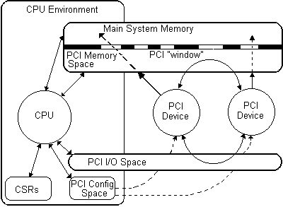
The CPU has visibility to the complete address space: it can access cached memory, CSRs as well as all the PCI memory, I/O, and configuration regions. See Figure 3-1.
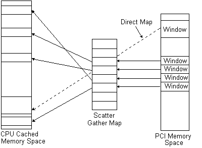
The PCI devices have a restricted view of the address space. Tthey can access any PCI device through the PCI memory or PCI I/O space, but they have no access to the PCI configuration space. Furthermore, the system restricts access to the system memory (for DMA operations) through five, programmable "windows" (i.e., memory regions) in the PCI memory space. (See figure below.)
DMA access to the system memory is achieved through "windows" in one of three ways:
The scatter/gather map allows any 8-KB PCI memory address region (page) to be redirected to any 8-KB cached memory page, as shown below.
PCI address Space |
The system generates 32-bit PCI addresses but accepts both 64-bit address (DAC, double address cycle) cycles and 32-bit PCI address (SAC, single address cycle) cycles. Main memory accessing is done as outlined below:
When the system is initialized by the SROM code, the windows are configured as follows:
| PCI Window | Assignment | Size | Comments |
|---|---|---|---|
| 0 | Scatter/Gather | 8MB | Not used by firmware. MEMCS disabled. |
| 1 | Direct Mapped | 1GB | Mapped to 0-1GB of main memory. |
| 2 | Disabled | ||
| 3 | Disabled | ||
CPU Address Space |
The following figure shows an overview of the mapping of the 40-bit processor physical address space into memory and I/O space addresses:
     39      34 33 32 31
+---+---+---+--+--+--+--+------------------------------+
|   |   |SBZ|  |  |  |  |                              |
+---+---+---+--+--+--+--+------------------------------+
      /\- - - - - - - - - +--------+
      |      0   0  x  x  |        |  8-GB Cached
      |                   +--------+      Memory
      |                   |        |
 <39>=0= Cached           |Reserved|
      |  Memory           |        |
      |  Space            |        |
      |                   |        |
      |                   |        |
      \/                  |        |
      - - - - - - - - - - +--------+ - - - - - -
      /\     0   x  x  x  |        | 80.0000.0000   /\
      |                   |        |                 |
      |                   | 16GB   |                 |
      |                   |        |            PCI Memory
      |                   |        |            Sparse Space
      |                   |        |            704-MB Max
      |                   +--------+                 |
      |      1   0  0  x  |  4-GB   | 84.0000.0000    |
 <39>=1= Uncached         |        |                 |
      |  I/O Space        +--------+                 |
      |      1   0  1  0  |  2-GB   | 85.0000.0000   \/
      |                   +--------+ - - - - - - -- - -
      |      1   0  1  1  |        | 85.8000.0000 PCI Sparse
      |                   |        |              I/O 64-MB
      |                   +--------+
      |      1   1  0  x  |        | 86.0000.0000 PCI Dense
      |                   |        |              Memory 4-GB
      |                   +--------+
      \/     1   1  1  x  |        | 87.0000.0000 PCI Config
      - - - - - - - - - - +--------+              CSRs, and
                                                    flashROM