| Updated: 05 November 1997 |
| Design of the 21174
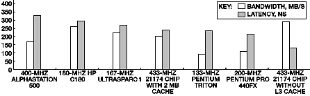
Memory Controller for DIGITAL Personal Workstations Reinhard C. Schumann Abstract DIGITAL has developed the 21174 single-chip core logic ASIC for the 21164 and 21164PC Alpha microprocessors. The memory controller in the 21174 chip uses synchronous DRAMs on a 128-bit data bus to achieve high peak bandwidth and increases the use of the available bandwidth through overlapped memory operations and simultaneously active ("hot") rows. A new prediction scheme improves the efficiency of hot row operations by closing rows when they are not likely to be reused. The 21174 chip is housed in a 474-pin BGA. The compact design is made possible by a unique bus architecture that connects the memory bus to the CPU bus directly, or through a QuickSwitch bus separator, rather than routing the memory traffic through the core logic chip. Introduction As microprocessor performance has relentlessly improved in recent years, it has become increasingly important to provide a high-bandwidth, low-latency memory subsystem to achieve the full performance potential of these processors. In past years, improvements in memory latency and bandwidth have not kept pace with reductions in instruction execution time. Caches have been used extensively to patch over this mismatch, but some applications do not use caches effectively.1 This paper describes the memory controller in the 21174 application-specific integrated circuit (ASIC) that was developed for DIGITAL Personal Workstations powered with 21164 or 21164A Alpha microprocessors. Before discussing the major components of the memory controller, this paper presents memory performance measurements, an overview of the system, and a description of data bus sequences. It then discusses the six major sections of the memory controller, including the address decoding scheme and simultaneously active ("hot") row operation and their effect on latency and bandwidth. Project Goals At the outset of the design project, we were charged with developing a low-cost ASIC for the Alpha 21164 microprocessor for use in the DIGITAL line of low-end workstations.2, 3 Although our goal was to reduce the system cost, we set an aggressive target for memory performance. Specifically, we intended to reduce the portion of main memory latency that was attributable to the memory controller subsystem, rather than to the dynamic random-access memory (DRAM) chips themselves, and to use as much of the raw bandwidth of the 21164 data bus as possible. In previous workstation designs, as much as 60 percent of memory latency was attributable to system overhead rather than to the DRAM components, and we have reduced that overhead to less than 30 percent. In addition, the use of synchronous DRAMs (SDRAMs) allowed us to provide nearly twice as much usable bandwidth for the memory subsystem and reduce the memory array data path width from 512 bits to 128 bits. Figure 1 shows the measured latency and bandwidth characteristics attainable with the 21174 chip in the DIGITAL Personal Workstation Model 433a and compares that data with measurements for several other systems. The STREAM (McCalpin) bandwidth measurements were obtained from the University of Virginia’s Web site.4 The memory latency was measured with a program that walks linked lists of various sizes and extrapolates the apparent latency from the run times.5 Note that the measured latency also includes the miss times for all levels of cache.
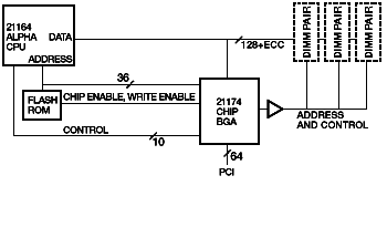
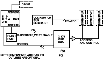
Figure 1 Despite our ambitious memory performance goals, our primary goal was to reduce cost. We considered eliminating the level 3 (L3) cache found in earlier DIGITAL workstations from our system design.6 Previous research indicated that a 21164 microprocessor-based machine without an L3 cache could achieve good performance, given good memory latency and bandwidth.7 Clearly, elimination of the L3 cache would reduce performance; we chose instead to retain the cache but as an optional feature. Typically, memory controllers used with Alpha microprocessors have used a data path slice design, with two or four data path chips connecting the CPU to the DRAMs. Early in our design process, we realized that these data path chips could be eliminated if the memory cycle time were made fast enough for noninterleaved memory read data to be delivered directly to the CPU. Previous designs used fast-page-mode DRAMs, but they could not be cycled quickly enough to provide adequate bandwidth from a 128-bit-wide memory. Consequently, a 256-bit or 512-bit memory data path was used in those designs, and data from the wide memory was interleaved to provide adequate bandwidth to the CPU. Recently, several types of higher bandwidth DRAMs have been introduced, including extended data out (EDO), burst EDO, and SDRAMs. All three memory types have adequate bandwidth for direct attachment to the data pins of the 21164, and all three are available at little or no price premium over fast-page-mode DRAMs. We eventually chose SDRAMs for our design because their bandwidth is better than that of the other two types, and because the industry-standard SDRAMs use a 3.3-volt interface that is fully compatible with the 21164 data pins 8 Fortuitously, SDRAMs were beginning to penetrate the mainstream memory market at the time we started our design, which provided assurance that we would be able to buy them in volume from multiple suppliers at little or no price premium. Although we eliminated the data path slices in the path from memory to the CPU, we still needed a data path from the memory to the peripheral component interconnect (PCI) I/O bus. When we started the design, it seemed clear that we would need multiple chips to accommodate the data path because of the 128-bit memory bus, 16-bit error-correcting code (ECC) bus, the 64-bit PCI bus, and their associated control pins. We planned to partition the design to fit into multiple 208-pin plastic quad flat pack (PQFP) packages. Our first design approach used two data path slices to connect the memory to the PCI bus and a third chip for the control logic. After a preliminary feasibility investigation with two ASIC suppliers, we decided to combine all three chips into one chip, using emerging ball grid array (BGA) packaging technology. Although a single chip would be more expensive, the elimination of two chips and more than 100 interconnections promised a reduction in main logic board complexity and size, thus partially offsetting the additional cost of the single chip design. In addition, the performance would be slightly better because critical paths would not span multiple chips and the design process would be much easier and faster. System Overview Figure 2 shows a system diagram for the cacheless design. Note that the memory array connects directly to the CPU. Figure 3 shows a configuration with an optional cache. In this configuration, a QuickSwitch bus separator isolates the CPU/cache bus from the memory bus. (A QuickSwitch is simply a low-impedance field effect transistor [FET] switch, typically several switches in one integrated circuit package, controlled by a logic input. In the connected state, it has an impedance of approximately 5 ohms, so it behaves almost like a perfect switch in this application.) From an architectural standpoint, it is not absolutely necessary to separate the buses when a cache is provided, but the bus separation substantially reduces the capacitance on the CPU/cache bus when the buses are disconnected, which speeds up CPU cache accesses significantly. As a side benefit, direct memory access (DMA) traffic to and from main memory can be completed without interfering with CPU/cache traffic. The arrangement shown in Figure 3 is used in the DIGITAL Personal Workstation, with the cache implemented as a removable module. With this design, a single mother board type supports a variety of system configurations spanning a wide performance range.
Figure 2
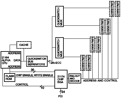
Figure 3 The memory controller also supports a server configuration, shown in Figure 4. In the server configuration, as many as eight dual in-line memory module (DIMM) pairs can be implemented. To cope with the additional data bus capacitance from the additional DIMMs, the DIMM portion of the data bus is partitioned into four sections using QuickSwitch FET switches; only one section is connected to the main data bus at any one time. In addition to the QuickSwitch bus separators, the server configuration requires a decoder to generate 16 separate chip select (CS) signals from the 6 CS signals provided by the 21174 chip.
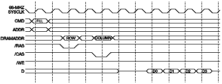
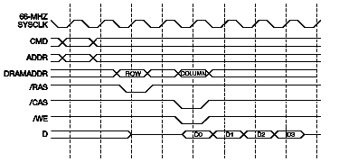
Figure 4 Data Bus Sequences The 21164 CPU has a cache line size of 64 bytes, which corresponds to four cycles of the 128-bit data bus. For ease of implementation, the memory controller does all memory operations in groups of four data cycles. Figure 5 shows the basic memory read cycle; Figure 6 shows the basic memory write cycle.
Figure 5
Figure 6 To provide full support for all processor and DMA request types, as well as cache coherence requirements, the memory controller must implement a large variety of data transfer sequences. Table 1 shows the combinations of data source and destination and the transactions that use them. All memory and cache data transfers are 64-byte transfers, requiring four cycles of the 128-bit data bus. All I/O transfers are 32-byte transfers, requiring two cycles. Table 1
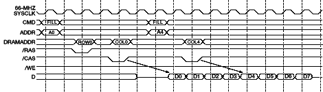
Notes The memory controller is designed to permit partially overlapped memory operations. The 21164 CPU can emit a second memory-fill request before the fill data from the first request has been returned. Figure 7 shows a timing sequence for two read commands to the same group of memory chips. Note that the second read command to the SDRAMs is issued while the data from the first read is on the data bus. The two read commands (four data cycles each) are completed with no dead cycles between the read data for the first read and the read data for the second read. For most other cases, the data cycles of adjacent transactions cannot be chained together without intervening bus cycles, because of various resource conflicts. For example, when the bus is driven from different SDRAM chips, at least one dead cycle between transactions is needed to avoid drive conflicts on the bus resulting from clock skews and delay variations between the two data sources.
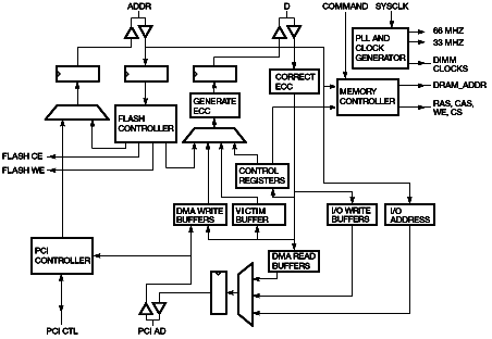
Figure 7 Memory Controller Components Figure 8 shows a block diagram of the 21174 chip. Table 2 gives an overview of key ASIC metrics. A discussion of the entire chip is beyond the scope of this paper, but note that there are two major control blocks: the PCI controller manages the PCI interface, and the memory controller manages the memory subsystem and the CPU interface. The memory controller has six major sections, as shown in Figure 9. The detailed functions of these components are described next.
Figure 8 Table 2
Figure 9 Memory Sequencer The main sequencer is responsible for overall transaction flow. It starts all transactions and issues all memory addresses and memory commands. Table 3 lists the transaction types supported by the main sequencer and the number of states associated with each type. Table 3
The data cycle sequencer is dispatched by the main sequencer and executes the four data cycles associated with each memory transfer. Although the data cycle sequencer is simple in concept, it must cope with a wide variety of special cases and special cycles. For example, in the case of reads and writes to flash read-only memory (ROM), stall cycles are needed, because of the slow access time and narrow data bus of the flash ROM. Table 4 gives the cycle types supported by the data cycle sequencer. Table 4
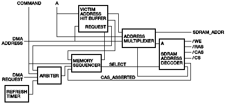
Some control signals from the memory sequencer are driven from the main sequencer, and some are driven from the data cycle sequencer. In addition, a number of control signals may be driven by either state machine. This is necessary because of pipelining considerations, as transactions are handed off from the main sequencer to the data cycle sequencer. For example, during a DMA write transaction, the DMA write data is selected on the internal data path multiplexer one cycle before it appears at the data pins, so the select signal for the internal multiplexer is driven by the main sequencer for the first data cycle of the DMA write and is then driven by the data cycle sequencer for three additional data cycles. The shared control signals are implemented separately in each state machine, and the outputs are simply ORed together. Address Multiplexer
Figure 10 Table 5
Note To further accelerate the address decoding, the input to the address multiplexer is sent directly from the address receiver ahead of the receive register, and a significant portion of the address decoding and multiplexing is completed before the first clock. SDRAM Address Decoder The opening and closing of rows (row access strobe [RAS]) and the launch of transactions (column access strobe [CAS]) is controlled separately for each DIMM pair by one of eight DIMM pair controllers. Each DIMM pair controller, in turn, contains eight bank controllers to control the four possible banks within each of the two groups of memory chips on the DIMM pair, for a total of 64 bank controllers. Figure 11 shows the details.
Figure 11 The address path and the launch of memory transactions are controlled by four signals from the main sequencer: SELECT, SELECT_FOR_READ, SELECT_FOR_WRITE, and SELECT_FOR_RMW. The SELECT signal directs the DIMM pair controllers to open the selected row. There are three basic cases. In the simplest case, the row is already open, and no further action is needed. In the second case, no row is open, and the DIMM pair controller must issue an activate command (or RAS) to the SDRAMs. In the most complex case, an incorrect row is open, and it must be closed by a precharge command before the correct row can be opened. The main sequencer asserts SELECT continuously until a data transfer is started. The DIMM pair controllers do not need to report the completion of the SELECT operation. They simply open the selected row as quickly as possible. However, if none of the DIMM pair controllers recognizes the address, a nonexistent memory status is signaled to the main sequencer. The SELECT signal can be issued speculatively. There is no commitment to complete a data transfer to the selected group of SDRAMs. For example, on a DMA read, SELECT is issued at the same time that a cache probe is launched to the CPU. If the CPU subsequently provides the read data, no memory read is needed, and the main sequencer simply deasserts SELECT. The main sequencer asserts a SELECT_FOR_READ, SELECT_FOR_WRITE, or SELECT_FOR_RMW signal when it is ready to start a data transfer. SELECT_FOR_RMW starts a normal read sequence, with the exception that the row hit predictor is ignored and the row is unconditionally left open at the end of the read, in anticipation that the next operation will be a write to the same address. (The subsequent write sequence would work properly even if the row were not left open, so this is strictly a performance optimization.) In response to a SELECT_FOR_x signal, the selected DIMM pair controller starts the specified transaction type as soon as possible. If necessary, the transaction start is delayed until the selected row has been opened. When the DIMM pair controller starts the data transaction (i.e., when it asserts CAS), it reports CAS_ASSERTED to the main sequencer. The memory controller provides almost unlimited flexibility for the use of different DIMM types among the three DIMM pairs (eight DIMM pairs in the server configuration). Table 6 gives the fields in the DIMM pair control registers. The DIMM pair size, as well as some SDRAM parameters, can be set individually per DIMM pair through these register fields. Table 6
Hot Rows The collection of hot rows can be regarded as a cache. This cache has unconventional characteristics, since the size and number of the hot rows vary with the type of SDRAM chip and with the number and type of memory DIMMs installed in the machine. In the maximum configuration, the cache consists of 24 cache lines (i.e., hot rows) with a line size of 16 kilobytes (KB), for a total cache size of 384 KB. Although the cache is not large, its bandwidth is 16 KB every 105 nanoseconds or 152 gigabytes per second. (The bus between this cache and main memory is 131,072 bits wide, not counting the 16,384 ECC bits!) Table 7 gives the state bits associated with each bank within each group of chips on each DIMM pair in the memory system. To keep track of the hot rows, a row address register is provided for each bank. There are 64 copies of the state given in Table 5, although only 24 of them are usable in the workstation configuration. Prior to each memory access, the row address portion of the current memory address is compared against the selected row address register to determine whether the open row can be used or whether a new row must be opened. (Of course, if the ROW_ACTIVE bit is not set, a new row must always be opened.) Table 7
As with any cache, the hit rate is an important factor in determining the effectiveness of the hot row cache. If a memory reference hits on an open row, latency is reduced due to the faster access time of the open row. However, if the memory reference misses on an open row, the row must first be closed (i.e., a DRAM precharge cycle must be done) before another row can be accessed. In the past, some memory controllers were designed to keep the most recently used row open in one or more memory banks. This scheme provides some performance benefit on some programs. On most programs, however, the scheme hurts performance, because the hit rate is so low that the access time reduction on hits is overshadowed by the time needed to close the open rows on misses. The memory controller uses predictors to guess whether the next access to a row will be a hit or a miss. If a hit is predicted on the next access, the row is left open at the end of the current access. If a miss is predicted, the row is closed (i.e., the memory bank is precharged), thus saving the subsequent time penalty for closing the row if the next access is, in fact, a miss. A separate predictor is used for each potential open row. There are 64 predictors in all, although only 24 can be used in the workstation configuration. Each predictor records the hit/miss result for the previous four accesses to the associated bank. If an access to the bank goes to the same row as the previous access to the same bank, it is recorded as a hit (whether or not the row was kept open); otherwise, it is recorded as a miss. The predictor then uses the four-bit history to predict whether the next access will be a hit or a miss. If the previous four accesses are all hits, it predicts a hit. If the previous four accesses are all misses, it predicts a miss. Since the optimum policy is not obvious for the other 14 cases, a software-controlled 16-bit precharge policy register is provided to define the policy for each of the 16 possible cases. Software can set this register to specify the desired policy or can disable the hot row scheme altogether by setting the register to zeros. The precharge policy register is set to 1110 1000 1000 0000 upon initialization, which keeps the row open whenever three of the preceding four accesses are row hits. To date, we have tested only with this setting and with the all-zeros and all-ones settings, and we have not yet determined whether the default setting is optimal. The adaptive hot row feature provides a 23-percent improvement in measured (i.e., best-case) memory latency and a 7-percent improvement in measured bandwidth against the STREAM benchmark, as reflected in Figure 1. Testing of the adaptive hot row feature shows an average performance improvement of 2.0 percent on SPEC95fp base and an average of 0.9 percent on SPEC95int base. The level of improvement varies considerably over the individual benchmarks in the SPEC suite, as shown in Figure 12, with improvements ranging from —0.6 percent to +5.5 percent.
Figure 12 For completeness, we also tested with the all-ones case, i.e., with the current row left open at the end of each access. This scheme resulted in a 5-percent performance loss on SPEC95fp base and a 2-percent performance loss on SPEC95int base. The row hit predictor is not as useful for configurations with an L3 cache, because the 21164 interface enforces a substantial minimum memory latency for memory reads to allow for the worst-case completion time for an unrelated 21164 cache access. In most cases, this minimum latency erases the latency improvement obtained by hitting on an open row. Victim Buffer Arbiter Table 8
Normally, DMA write requests, L3 cache victims, and refresh requests are low-priority requests. However, a second request of any of these types can become pending before the first one has been serviced. In this case, the priority for the request is increased to avoid unnecessary blockage or overruns. Refresh Controller Cache Coherence
Figure 13 If the DMA write covers an entire cache line, the memory controller requests that the CPU invalidate the associated entry, and the DMA data is then written directly to memory. If the write covers a partial cache line, a cache lookup is performed; on a hit, the cache data is merged into the write buffer before the data is written to memory. If the cache misses on a partial line write, two outcomes are possible: If each 128-bit memory cycle is either completely written or completely unchanged, the data is written to memory directly, and the write to the unchanged portions is suppressed using the data mask (DQM) signal on the memory DIMMs. If there are partially written 128-bit portions, the full cache line is read from memory and the appropriate portions are merged with the DMA write data. Cache Flushing In addition to the fake memory, the memory controller provides a cache valid map that can make cache flushing faster when the cache is lightly used. The cache valid map is a 32-bit register, in which each bit indicates whether a particular section of the cache has been (partially) filled. When a cache fill request is processed, the memory controller sets the corresponding bit in the cache map register. The bits of the register can be individually reset under program control. To use this feature, the cache must first be completely flushed and the register reset to zeros. Thereafter, the cache map register reflects which sections of the cache can potentially contain dirty data. During a subsequent cache flush, the flush algorithm can skip over those sections of the cache whose corresponding bits in the cache map register have not been set. This feature is useful primarily for cache shutdowns that occur between keystrokes, i.e., when the system is nearly idle but has frequent, short bursts of activity to service keyboard input, clock interrupts, modem receive data, or similar workloads. Conclusion The 21174 chip provides a cost-effective core logic subsystem for a high-performance workstation. The use of SDRAMs, high-pin-count BGA packaging, and hot rows make possible a new level of memory performance, without the need for wide memory buses or a complex memory data path. Acknowledgments I would like to express my appreciation to Jim Delmonico, Jeff Forsythe, Frank Fuentes, Paul Hill, Kenny House, Mark Kelley, Yong Oh, Rob Orlov, Rajen Ramchandani, Don Rice, Dean Sovie, and Ken Weiss, who gave a year of their lives to implement and simulate the 21174 chip and who made it work on the first pass! I would also like to thank Lance Berc, who provided most of the latency data, and Greg Devereau, Arlens Barosy, and John Henning, who provided other performance measurements. References 1. S. Perl and R. Sites, "Studies of Windows NT Performance using Dynamic Execution Traces," Proceedings of the Second USENIX Symposium on Operating Systems Design and Implementation (1996). 2. J. Edmonson et al., "Internal Organization of the Alpha 21164, a 300-MHz 64-bit Quad-issue CMOS RISC Microprocessor," Digital Technical Journal, vol. 7 no. 1 (1995): 119–135. 3. Digital Semiconductor 21164 (366-MHz Through 433 MHz) Alpha Microprocessor (Maynard, Mass.: Digital Equipment Corporation, Order No. EC-QP99A-TE, 1996). 4. J. McCalpin, "STREAM: Measuring Sustainable Memory Bandwidth in High Performance Computers," http://www.cs.virginia.edu/stream/ (Charlottesville, Virg.: University of Virginia, 1997). 5. L. Berc, "Memory Latency," Digital internal Web pages, September 1996. 6. J. Zurawski, J. Murray, and P. Lemmon, "The Design and Verification of the AlphaStation 600 5-series Workstation," Digital Technical Journal, vol. 7 no. 1 (1995): 89–99. 7. D. Conroy, "Cacheless Ev5," Digital internal document. 8. KM44S4020B/KMS4021B CMOS SDRAM Data Sheet (Seoul, Korea: Samsung Electronics Company, Ltd., 1996). Biography
Reinhard C. Schumann Trademarks DIGITAL is a trademark of Digital Equipment Corporation. QuickSwitch is a registered trademark of Quality Semiconductor, Inc. SPEC is a registered trademark of the Standard Performance Evaluation Corporation. |
Legal |
|||||