| Updated: 05 November 1997 |
| DIGITAL Personal
Workstations: The Design of High-performance, Low-cost
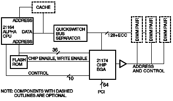
Alpha Systems Kenneth M. Weiss and Kenneth A. House Abstract The new DIGITAL Personal Workstations for Windows NT (a-series) and DIGITAL UNIX (au-series) incorporate a 21164 Alpha microprocessor, a highly integrated core logic interface, synchronous main memory and cache, and commodity PC parts. The traditional core logic chip set has been designed as a single-chip ASIC. The high-performance uniprocessor workstation includes a low-cost interrupt scheme, tight timing control of clocks for maximal performance, and a flash ROM interface. Introduction In 1995, DIGITAL began development of a low-cost system implementation of the 21164 microprocessor, incorporating emerging memory technologies to improve system performance. This paper discusses the major architectural and design features of the DIGITAL Personal Workstation a-series and au-series, low-cost, high-performance systems powered by the 21164 Alpha microprocessor. It focuses on some of the unusual design features incorporated into the new core logic chip, the 21174 application-specific integrated circuit (ASIC). The paper also addresses a novel clock distribution strategy with feedback for skew reduction, a low-cost interrupt scheme, and a capability to boot directly from reprogrammable flash read-only memory (flash ROM). The original project was to build a platform for the DIGITAL Personal Workstation running the Microsoft Windows NT operating system. This system is designated as the a-series (e.g., 433a, 500a, 600a, e tc.). Soon after shipping this product, the same hardware components were qualified and shipped with the DIGITAL UNIX operating system as the au-series (e.g., 433au, 500au, 600au, etc.). Motivation For years, main memory technology has been based on fast-page-mode dynamic random-access memory (DRAM). In the personal computer (PC) market, fast-page DRAMs were soldered onto single in-line memory modules (SIMMs). Although the access times of these memories have been decreasing (i.e., 80 nanoseconds [ns]-> 70 ns -> 60 ns), improvements in CPU technology and core logic chip sets have evolved more rapidly. In 1995, the PC market began to move to extended data out (EDO) memories, which were roughly twice as fast as the fast-page memories, and burst EDO was on the horizon. Several DRAM vendors began to talk about new synchronous DRAMs (SDRAMs), which provided even greater performance and the promise of reaching commodity price levels by 1997. Reduced instruction-set computers (RISC) in general, and Alpha machines in particular, require faster memories. Alpha CPUs run much faster than the leading complex instruction-set computer (CISC) (e.g., Intel x86) processors and need a faster path to memory to keep pace with the demands for instructions and data. DIGITAL and other Alpha system developers have been satisfying this need with wider memory buses; for instance, the AlphaStation 500 and AlphaStation 600 series systems have a 256-bit memory bus, four times wider than the typical 64-bit bus on leading-edge PCs. Also, the larger external caches on DIGITAL’s systems reduce the memory bandwidth requirements by keeping frequently used data local to the processor. This advantage, however, was shrinking for two reasons: faster memories were being introduced for PCs, and low-cost systems with 256-bit memory buses and large external caches are difficult and expensive to build. It became clear that a new system design was required, one that could take advantage of the new memory technologies and one that could be implemented at a lower cost. This, in turn, would require the design of new core logic that would function as the CPU-to-memory interface. Although the system design was planned to take advantage of higher-performance memory technologies, the primary emphasis was placed on lowering system cost. The design team had a multipronged approach to meeting this goal. In addition to following the established Design for Manufacturing techniques and selecting low-cost components, we focused on creating a highly integrated, low-cost core logic ASIC. Design Overview In traditional system-level designs, the memory data bus goes through the core logic chip set.1–3 This approach isolates the CPU side of the data bus from the large electrical load of the memory chips and interconnect, thereby allowing the CPU to access its cache more quickly on the lightly loaded bus. This approach also gives the chip set access to the memory data for transfers to and from the I/O bus, while at the same time allowing the CPU concurrent access to the cache. Finally, this design allows the memory and CPU buses to be different widths, with the core logic chip set functioning as a multiplexer/demultiplexer between the two different buses. However, there are disadvantages to this scheme. For example, each data line requires two pins in the chip set (and more, for the extra power and ground lines), significantly increasing the size and cost of the chip set. Also, memory latency is increased by the additional time needed to get data through the chip set to the CPU, which hurts performance. In our design, the memory-to-CPU data bus goes by the core logic chip rather than through it. The data bus attaches to only one pin per bit. Figure 1 shows a simple block diagram of the system. To isolate the CPU and the backup cache (B-cache) from the memory bus, we used a separate bank of QuickSwitch bus separators. These bus separators are large complementary metal-oxide semiconductor (CMOS) pass transistors, which appear as either short circuits or open circuits, depending on the state of their enable pin. In the open mode, they allow the CPU to access its B-cache in isolation. When closed, memory data travels through the bus separator with a small (250 picoseconds [ps] through 5 ohms) propagation delay, thus avoiding the latency/performance penalty of going through the chip set.
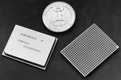
Figure 1 Incorporating high-volume commodity parts into a design is less expensive than adding extra pins to a relatively low-volume, high-pin-count ASIC. The small size of the bus separators allows them to be placed closer to the CPU and cache for a shorter, quicker CPU interface. Finally, a low-end cacheless configuration can be built without them. Another feature of our CPU-to-memory interface is that the "chip set" is a single chip. Although the original design called for three chips, new packaging technologies were making larger pin-count devices more affordable and manufacturable.4 We compared various implementations from several ASIC vendors and eventually chose a single-chip implementation. (The Technology Choices section in this paper discusses the details.) Finally, making the B-cache optional is a new feature for Alpha workstations. Recent Alpha workstations have been hampered by the relatively slow, fast-page-mode main memory coupled to an increasingly high-speed processor. With this imbalance, a large external B-cache has been essential to speed up CPU accesses by reducing average memory latency and memory bandwidth requirements. We investigated an internal research project in which very fast memory systems were coupled to the 21164 CPU. An experimental cacheless machine used a 512-bit-wide (fast-page mode), low-latency memory system and performed very well on many memory-intensive benchmarks. This work helped inspire the cacheless concept for the 21164 CPU; however, the performance of the experimental system was relatively mediocre on some benchmarks (cache intensive), which led us to conclude we needed to offer an optional B-cache as well. Technology Choices As mentioned previously, system development was concurrent with some significant changes to main memory technology. Our main issue was determining which of the new technologies—EDO, burst-EDO, synchronous, or Rambus—would be the next standard in the commodity PC business. This was a key decision: a wrong choice could lead to prohibitively expensive memory, effectively making the system a high-cost platform. Our first analysis pointed to burst-EDO, since it was the most compatible with the existing fast-page memories. Several months into the design, however, many of the key memory vendors abandoned burst-EDO in favor of SDRAM. With help and advice from memory component engineers within DIGITAL, we switched over to synchronous memory. (This was a fortuitous decision, since commodity PC platforms are now moving to SDRAM, assuring its place as the next high-volume memory technology.) From our first look at memory bandwidth with the new SDRAM, we realized that designing a B-cache to keep pace with it would be difficult. The system’s memory, running at 66 megahertz (MHz), would have more bandwidth than any other Alpha workstation’s B-cache. In fact, it was difficult to design a B-cache that was not the limiting factor in memory bandwidth. From the cache technologies supported by the 21164, we selected synchronous flow-through static RAM cache parts. Although this choice was expensive, an external cache that significantly increased performance was imperative for our product. Our next major decision was choosing our ASIC technology and package. After evaluating quotes for different chip configurations from several vendors, we selected the single-chip implementation in a 474-pin ceramic ball-grid array package (BGA) offered by International Business Machines Corporation (IBM). The package measures only 1.0 by 1.25 inches and uses flip-chip technology, in which the die is bonded directly to the ceramic package without lead wires. The ceramic carrier is a seven-layer design that connects the die pads to a 50-mil (.050-inch) BGA for assembly onto the printed circuit board. Contrary to our initial concern, the package was not too difficult to route on the printed circuit board. In addition to its small size and reasonable price, the package offered low inductance (short) power, ground, and signal connections, which provided for good signal integrity. Figure 2 shows a photograph of the ASIC package.
Figure 2 Most of the other technology choices we faced do not warrant specific mention, except for the system enclosure. Since our system was destined to become a DIGITAL Personal Workstation, it had to be highly compatible with DIGITAL’s leading-edge Intel processor-based workstation (i-series). The use of common components makes it easier for development, manufacturing, distribution, and service. As a result, we had to fit our system into an existing DIGITAL PC enclosure, use the same power supply, have similar option configurations, and so forth. This constraint had both good and bad ramifications, which we discuss in a later section, Logic Partitioning and Enclosure. System Clocks In Zen and the Art of Motorcycle Maintenance, Robert M. Pirsig argues that one can look at a complex system from many different viewpoints.5 In that spirit, the logic/system design is illuminated by its clocking details. We will touch on the major points of interest in this section. Clocking Overview For example, a 600-MHz CPU would have its divide ratio set to nine, yielding a 66.6-MHz SysCLK, whereas a 500-MHz system would set the ratio to eight for a 62.5-MHz system clock. A programmable, delayed version of SysCLK, SysCLK_2, also is available from the 21164 CPU and is used as the main clock source in the 21174 core logic ASIC. In the system, SysCLK_2 is delayed nearly a full clock cycle, so that by the time it reaches the core logic ASIC, it arrives roughly coincident to SysCLK. Clock Divisors and Clock Domains
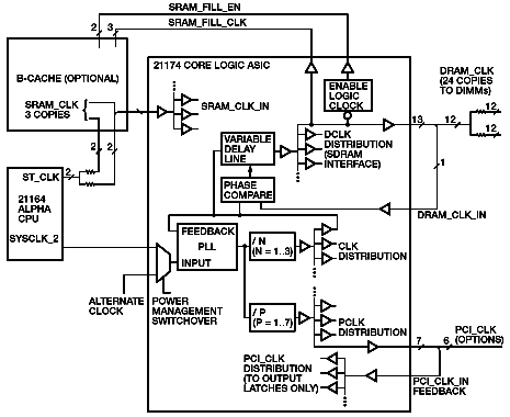
Figure 3 The external PCI bus is specified to run as high as 33.3 MHz, a limit required for successful operation of industry-standard I/O option cards. The core logic ASIC runs its PCI interface at PCI speeds and thus needs a separate 33.3-MHz PCI clock. Since SysCLK is running at 66.6 MHz, we can simply divide it by two to arrive at a nominal 33.3-MHz PCLK. In addition, the core logic ASIC has a clocking system capable of running these clock domains at many different ratios. It allows for operation faster than 66.6 MHz and includes divide ratios to generate PCI clocks that do not exceed 33.3 MHz. For example, one interesting frequency for the core logic ASIC is 83.3 MHz. With the CLK divisor set at two (N = 2 in the drawing), the output of the PLL will be running at 166.6 MHz. With the PCLK divider at five (P = 5), the resultant PCI clock rate becomes 33.3 MHz. The dividers are clocked by both a positive PLL clock and an inverted PLL clock, allowing for symmetry in the output clocks for odd divisors. Any significant drift or skew in the two major clocking domains, CLK and PCLK, would result in timing problems (mostly hold time) as signals cross from one domain into the other. Therefore, these clock domains had to be in nearly perfect alignment. To achieve this, we ensured that the clock distribution trees had tightly controlled delays, that the core of the clock dividers was implemented structurally (at the gate level), and that all associated logic was balanced in the layout. Then we did a complete timing analysis to ensure proper operation. So, why bother with all this? An odd frequency mix such as this one is often achieved with asynchronous boundaries and often with much pain. Asynchronous interfaces are difficult to design and to verify. Furthermore, the transitions across these boundaries can often be slow and add data latency. The 21174 core logic ASIC design allows for flexible operation frequencies, while maintaining a synchronous design. The 21174 ASIC was designed to accommodate several different frequency combinations, and the internal data and control signals that cross the CLK to PCLK boundary were implemented accordingly. As the design progressed, however, we found it was too difficult to run the external memory and B-cache subsystems faster than 66.6 MHz, given the current technologies. As an unfortunate result, these features have not yet been used. SDRAM Clock Generation Like other large ASICs, the 21174 has a large timing variation on its I/O cells. Unlike other large ASICs, it employs a novel feedback circuit that automatically compensates for delay uncertainty and ultimately delivers tightly aligned clocks. Figure 4 shows some details of this circuit, which is used to generate the main memory clock, DRAM_CLK. This clock originates inside the ASIC as a copy of the tightly aligned internal clock, CLK, which is then distributed through a variable delay line. The resultant delayed clock is then sent, in multiple copies, out of the chip to the SDRAM memory dual in-line memory modules (DIMMs).
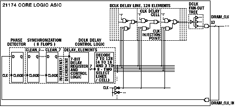
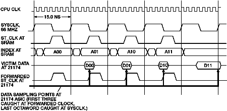
Figure 4 The variable delay line consists of 128 independent delay cells, which have a delay of roughly 200 ps each. Each delay cell maintains the same polarity of the clock but inverts it twice to compensate for different gate rise and fall times. By adjusting the number of delay cells in the path, the 21174 ASIC can control the timing of the output clock. With that accomplished, the core logic ASIC must now determine and control the number of delay elements used. As Figure 4 shows, the 21174 ASIC generates 13 identical copies of the DRAM clock; 12 copies go to the memory arrays (two per DIMM). The thirteenth copy feeds back into the ASIC. Conceptually, the extra copy goes to a phase detector, which compares it against its own internal clock, CLK. If the sampled DRAM_CLK leads CLK, then the phase detector automatically increases the delay of the DRAM_CLK variable delay line by adding one more element to the delay chain. Conversely, if DRAM_CLK trails CLK, one element of the variable delay line is removed. The alignment circuitry continues to add (or remove) one delay element until the clocks are slightly past the optimal alignment; at that point, it then subtracts (or adds) a delay element. The circuit thus brings the clocks close to alignment and then toggles back and forth by one delay element, which adds slight but acceptable jitter to the clocks. The phase detector is logically a D flip-flop, with CLK driving its clock input and DRAM_CLK as its data input. The two output states thus represent "CLK leads DRAM_CLK" and "CLK trails DRAM_CLK." The circuit pings back and forth between the final two delay elements because the phase detector does not directly indicate that clocks are in alignment. Also, once the clocks are in alignment, timing could drift because of delay changes caused by temperature or voltage variations, which require the circuit to be left on. The goal of this clock circuit is to precisely align the phase detector’s clock, CLK, with its data, the input copy of DRAM_CLK. This nearly guarantees that the flop will be operating in violation of its normal setup-and-hold timing window because its data are changing at the clock edge. (State elements like to have a setup-and-hold window around the clock where the data is stable at either a 0 or a 1.) This violation can cause both uncertainty in its output state, as well as problems with metastability in the flip-flop. Fortunately, we were able to use a special metastable hardened flip-flop in IBM’s CMOS5 library as one of the phase detectors in the 21174 ASIC. (The circuit offers two phase detectors; each is implemented with a different flop and is selectable during power-up.) Also, the output of the phase detector was sent through seven more metastable flops in series. These flops clean up and synchronize any metastable state that may occur and send a clean output to the variable delay line control circuitry. Although ASICs can have a large variation in output delay from chip to chip and for different voltages and temperatures, cell delays are correlated to a large degree within a chip. In short, if one I/O cell in a chip is running fast, they will all be running fast. Thus, by lining up one of the DRAM CLKs, they are all in rough alignment with it. Although this compensates for the output buffer delay, the rest of the clock feedback path is not automatically correlated. The external printed circuit board wiring, however, has relatively little skew contribution because propagation delays in etch are relatively constant and easily calculated. (The wiring will correlate to the etch delay of the other clocks going to the DIMMs.) The input buffer cell delay of the feedback clock is not correlated, but this is relatively fast and not consequential. Some additional aspects of the circuitry are worth mentioning. For example, in the 21174 ASIC implementation, the automatic delay alignment circuitry can be selectively enabled or disabled by software (it powers up disabled). Software can force the number of delay elements. This allows us to derive more elaborate schemes of fine-tuning the SDRAM clocks, such as advancing the clock when there are more DIMMs in the system and retarding it when there is light memory bus loading. Note that other nonrelated signals that use the same internal DCLK and the same I/O cell type are delay correlated to the DRAM clock signals. Several other signals to the B-cache, which needed a tight timing relationship to the memory, were generated in this fashion. Also, most of the memory interface signals are generated from DCLK, which made the normally difficult job of interfacing to the high-speed memory a relatively easy one in terms of timing. The clock-alignment circuitry was one of the first things we checked after we powered on the first system. As soon as we wrote the bit to enable the auto alignment feature, the clocks snapped into the calculated/expected positions. B-Cache Clocks Each of the two ST_CLK pins on the 21164 CPU are split into two separate copies through a resistor-splitting network. The resultant four copies of ST_CLK route to the B-cache module. Three of these copies are available for the synchronous static RAMs on the cache module, and the fourth copy routes to the 21174 core logic chip. The current implementation of the B-cache module uses only one copy of ST_CLK, which is buffered and sent to the individual synchronous static RAM chips. The system platform delivers three additional copies of the DRAM_CLKs to the B-cache module, called SRAM_FILL_CLK, which also take advantage of the DRAM_CLK alignment just described. These clocks can be used to clock the synchronous static RAMs during memory fills to give the least amount of clock skew between the memory and the cache. A separate set of time-aligned signals, SRAM_FILL_EN, can be used to switch between the ST_CLK and SRAM_FILL_CLK sources. The 21174 ASIC implements a victim buffer for dirty (updated) B-cache data being evicted to memory.4 To optimize victim eject timing to the core logic ASIC, the system uses a forwarded copy of the ST_CLK clock sourced from the 21164 CPU and sent to the 21174 ASIC (see Figure 3). This clock, SRAM_CLK_IN, works similarly to the 21164 CPU’s wave pipeline feature and allows ejection of a victim from the cache to the 21174 ASIC in five SysCLK cycles rather than the eight cycles it would have taken without it.6 For flexibility in future B-cache upgrade cards, this clock routes through the B-cache module, which allows its timing to be fine-tuned for the specific B-cache module parts. Figure 5 shows this timing.
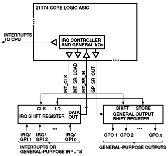
Figure 5 Flash ROM and Boot The 21174 core logic ASIC implements the boot code, the console firmware, and the nonvolatile RAM (NVR) interface in the system, another example of a system feature that was integrated into the core logic ASIC. A single, one-megabyte (MB) flash ROM holds thepower-on self-test (POST), two 16-kilobyte copies of NVR, and the AlphaBIOS and SRM consoles. These separate components were combined to save board space that would have been used by separate parts: serial ROM, NVR, and two programmable ROMs. The more highly integrated design also reduced costs, which was consistent with our design goals. The single flash ROM is connected on the address bus between the CPU and the core logic ASIC (see Figure 1). By placing these critical software components logically closer to the CPU, rather than on the I/O bus, we provided a greater ability to diagnose the system when not all of its parts are working. Flash ROM was used to ease updating the firmware in the field, allowing upgrades from a floppy diskette (possibly downloaded from the DIGITAL Web site). The initial power-on boot sequence on the system is also unique among Alpha workstations. All Alpha CPUs can use a serial ROM to load the primary instruction cache (I-cache) at power-on; once the I-cache is full, execution begins. Alternatively, the 21164 CPU can bypass the serial ROM load and begin executing directly from memory. These instruction stream (I-stream) accesses miss in the CPU’s empty internal caches, causing external fills. The system implements this form of power-on, using the core logic ASIC to intercept I-stream fills and retrieve the data from flash ROM. This saves the board space and cost associated with either a specialized serial ROM part or the logic to serialize a standard ROM. At initial power-on, the core logic ASIC interprets CPU requests for reads from addresses 00.0000.0000 through 00.03FF.FFFF as requests for data from the flash ROM. The transaction begins with a read_block_miss command from the CPU. The core logic ASIC asserts cack_l to acknowledge the command and then asserts addr_bus_req to request the private use of the CPU-to-21174 ASIC address bus. It then issues reads to the flash ROM by passing address and control information on the now-reserved address bus. Since the core logic ASIC owns the bus, it does not have to adhere to conventional usage: the address bits are free for reassignment. Addr<31:12> is used as the byte address into the flash ROM; the eight-bit datum is returned on addr<11:4>. Sixty-four successive bytes read from the flash ROM are packed into a buffer in the core logic ASIC and returned to the CPU to complete the original fill request. There are two different address ranges used for flash ROM fills: one starting at address 00.0000.0000 (to allow power-on from code in flash ROM) and another at address 0F.FC00.0000 (above any possible memory). Both ranges access the same flash ROM data. POST code quickly jumps to the high address range, disabling the low range and freeing those addresses for use by memory before it begins to size the DIMMs. Byte read and write access to the flash ROM is also supported for access to NVR and for updating the firmware. This address range starts at C7.C000.0000. Only two function-specific pins on the core logic ASIC are used for the flash ROM interface, write enable (flash_we_l, deasserted during fills) and chip enable (flash_ce_l). The flash ROM’s output enable is controlled through an address line, addr<39>. A socket is provided on the system mother board to allow for the use of a real serial ROM part. The circuitry automatically detects the presence of a serial ROM and will direct the 21164 CPU to boot from the serial ROM port if the part is installed. This allows a serial ROM to be used in case of damage to, or inadvertent corruption of the flash ROM. This feature is also useful for module-level debug, because serial ROM parts with specific test scripts can be made. Interrupt Controller The system provides separate inputs for every possible PCI interrupt (Figure 6), avoiding the problems that shared interrupts bring: longer latency, unnecessary I/O, configuration restrictions, and so forth. We implemented a serial I/O scheme to handle PCI interrupts and miscellaneous I/O. This has the advantage of bypassing the Industry Standard Architecture (ISA) interrupt handlers entirely, except for true ISA interrupts. Many previous designs run the PCI interrupts through the PCI-to-ISA bridge, which requires additional I/O to determine the device that needs attention. In the design of the system, we tried to avoid the need for time-wasting I/O accesses wherever possible, moving the access closer to the CPU if it could not be eliminated entirely. Further down the hierarchy of buses (CPU to PCI to ISA), latencies increase and the possibility of contention rises. For a high-frequency RISC CPU such as the 21164, stalling the CPU has a significantly higher penalty than for slower processors. The core logic ASIC uses only three pins to control external shift registers for interrupts and general-purpose inputs and incorporates a fourth pin that handles general-purpose outputs (such as control bits or light-emitting diodes [LEDs]). The external logic is shown in Figure 6, where int_clk is the shift clock into the external shift registers, int_sr_load_l is the load pulse for both input and output, int_sr_in is the serial input stream, and the serial output is on gp_sr_out.
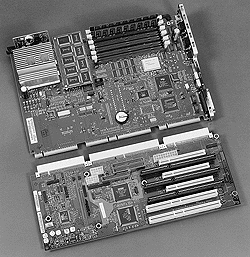
Figure 6 Inside the core logic ASIC, we used several registers in the interrupt controller. All interrupts and general-purpose inputs are readable in the 64-bit int_req register, letting the interrupt dispatch code determine relative priorities. A corresponding int_mask enables or disables each input as an interrupt. To save external inverters, an eight-bit register (int_hilo) is used to change the polarity of individual inputs in the low byte (inputs are assumed to be active-low signals, but some inputs are contrary). Another eight-bit register is int_route, which can selectively route some inputs to different interrupt lines on the CPU; although most interrupts are delivered on the CPU’s irq_h<1> line, this feature allows the clock to come in at a higher priority and other inputs to cause a machine check, a power-fail interrupt, or a halt condition. The interrupt controller can be configured for the number of bits used, in blocks of eight, for as many as 64 bits. We set the interrupt controller for 32 bits, implemented as four, cascaded, eight-bit parallel-to-serial shift registers and two serial-to-parallel parts, which was sufficient for the system. The timing of the shift clock is adjustable to balance the cost of the shift registers against the interrupt latency. These two parameters are maintained in the int_cnfg register. A small additional interrupt latency was introduced by the serial interface. We judged this to be an acceptable compromise, since we eliminated several I/O accesses per interrupt. Note that when multiple interrupts occur within the same shift cycle, all are available to the CPU’s interrupt dispatch routine simultaneously, with only one read of the core logic ASIC’s int_req register. Soft Reset The core logic ASIC generates and drives all the system reset lines, including its own. It receives a DC_OK (DC power supply levels charged and okay) signal from an external voltage monitor, waits for its internal PLL to lock, and then delays for a programmable (by means of external pull-up/pull-down resistors) number of cycles before deasserting reset to the system. Also, the core logic ASIC implements a soft reset feature whereby software can reset the entire machine, with the exception of a few key registers in the core logic ASIC. This allows software to reconfigure certain key CPU and core logic ASIC clocking parameters, hit reset, and acquire the new timing. For example, the state of the CPU’s interrupt pins during system reset determines the external clock characteristics of the 21164, such as the SysCLK divide ratio and the SysCLK_2 delay (mentioned earlier). At power-on, these are set by pull-up and pull-down resistors on the module to the slowest speed. After software establishes the CPU’s operating frequency, it can configure the interrupt logic to drive these lines to the correct value and reset the machine. The next time the CPU restarts, software recognizes the right clock parameters and continues with the boot code. Embedded Real-time Counter and Timer Interrupt A 64-bit real-time counter in the rt_count register, ticking with the system clock, is useful for microscopic timing measurements. The core logic ASIC provides an int_time alarm register to interrupt the CPU at specific values of rt_count. The system uses the real-time clock in one of its peripheral I/O chips (super I/O) for the system timekeeper, bypassing the ISA interrupt controller and bringing its interrupt straight to the input shift registers, which saves PCI bandwidth and processor cycles. I2C Interface Two pins on the core logic ASIC were set aside for general-purpose inputs or outputs, under total software control. In the system, these are used by software to implement an I2C (inter-IC) interface for clock and data. This serial interface allows input of static configuration data from the six DIMMs and the B-cache module. At power-on, firmware reads information from small, serial electrically erasable read-only memories (EEROMs) on each of these modules. Thus the interface can easily establish system configuration as well as set up memory and cache timing. The DIMM I2C ROM contents are defined by the Joint Electron Devices Engineering Councils (JEDEC) standards and can be programmed in place. Since the I2C data is read only once at power-on, it was not important to make this interface fast. Consequently, it was implemented as a "bit-bang" port, in which each transition on each line is controlled by firmware accesses to logic registers. Firmware is responsible for timing of the protocol’s clock and for setup and hold of the data. Also, firmware handles deserialization (byte packing) of the incoming data stream. Logic Partitioning and Enclosure Most of the system logic is partitioned onto two boards: a riser card and the mother board (often referred to as the main logic board [MLB]). The riser card is used for all components common across the DIGITAL Personal Workstation line; it includes five option slots, audio, and Ethernet logic. All internal cables connect to the riser, which is intended to be common between the platforms. Figure 7 shows a photograph of the system logic.
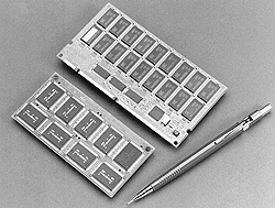
Figure 7 Because of the shared riser, the a-series and i-series systems have much in common. For example, they use the same PCI–PCI bridge chip, with identical option slot layouts. The CD-quality audio and 10/100 megabits per second Ethernet logic are common, as are the bulkhead cards for these signals. The MLB contains the CPU, core logic chip (set), cache, memory, and miscellaneous external connectors. Figure 8 shows the optional B-cache module and a custom-designed memory DIMM. Because there are no internal connections, it is easy to remove an Intel MLB and replace it with an Alpha board.
Figure 8 In a design compromise, we added a PCI–IDE chip on the MLB to match the partitioning dictated by existing i-series machines, which have integrated device electronics (IDE) built into their core logic. The natural place for such a device would have been on the riser card. A graphics controller was not embedded so the customer could select from adapters of varying cost and performance. For those users with a CPU-intensive application who do not need high-quality, high-performance graphics, a less expensive adapter may be adequate. Demanding users, such as those doing mechanical computer-aided design (CAD), will find that the high-end graphics cards offer a significant boost in quality and performance. A small computer systems interface (SCSI) controller is provided as a PCI option card for several reasons. First of all, it was more expensive to embed SCSI and provide a bulkhead card for an external connection. Using an option card allows us to move to better SCSI solutions as they become available. Customers with a light disk I/O load may choose to use a less expensive IDE hard disk. Although there were many benefits to sharing so many components between the a-series (Alpha) and the i-series (e.g., Intel x86), the development process was not conflict-free. The Alpha development team faced several significant problems. Because the i-series development started sooner, much of the feature set and logic partitioning was already committed before we had a chance to participate in the design. The original enclosure proved to be inadequate, and we had to make changes for cooling, FCC containment, and mechanical support of option cards. Also, there were difficulties that reflected the different market requirements for PCs and workstations. For instance, an external HALT button, which forces a running machine to the firmware console, is a standard feature in the UNIX and OpenVMS markets but is missing in the DIGITAL Personal Workstation. Results and Summary The 21174 core logic ASIC was implemented as a standard-cell ASIC design and uses about 320,000 cells (250,000 gate equivalent) on a 7.2-millimeter square die, routed in five layers of metal. The design uses 384 signal pins in a 474-pin ceramic BGA package; the remaining pins are used for power and ground. The DIGITAL Personal Workstation a-series and au-series include the 21164 Alpha CPU, the 21174 core logic ASIC, synchronous DRAM, and a 64-bit PCI bus. Acknowledgments The authors would like to thank all the people who contributed their skills and time to the successful design of the Alpha microprocessor-based personal workstations known internally as the PYXIS/MIATA/MX5 projects. Special thanks are due to the core engineering design, development, and debug team: Arlens Barosy, Frank Calabresi, Jim Delmonico, Jeff Forsythe, Frank Fuentes, Paul Hill, Bob Hommel, Mark Kelley, Yong Oh, Rob Orlov, Rajen Ramchandani, Dan Riccio, Don Rice, Ty Rollin, Arnold Smith, and Dean Sovie. Many thanks also are in order for our qualification team, including Bill Grogan, Bob O'Donnell, Phil Puris, Lynne Quebec, and Matt Twarog; our engineering manager, Fred Roemer; our product manager, Keith Bellamy; and our group’s technical writer, Carmen Wheatcroft. We also wish to acknowledge Dave Conroy from the Systems Research Center for his work on the cacheless machine. Finally, special acknowledgment is due to Reinhard Schumann, who contributed an extraordinary amount of inspiration to the design and perspiration to the implementation. References 1. S. Nadkarni, W. Anderson, L. Carlson, D. Kravitz, M. Norcross, and T. Wenners, "Development of Digital’s PCI Chip Sets and Evaluation Kit for the DECchip 21064 Microprocessor," Digital Technical Journal, vol. 6, no. 2 (Spring 1994): 49–61. 2. J. Zurawski, J. Murray, and P. Lemmon, "The Design and Verification of the AlphaStation 600 5-series Workstation," Digital Technical Journal, vol. 7, no. 1 (1995): 89–99. 3. Pentium Processors and Related Products (Mt. Prospect, Ill.: Intel Corporation, Order No. 241732-002, ISBN 1-55512-239-6, 1995). 4. R. Schumann, "Design of the 21174 Memory Controller for DIGITAL Personal Workstations," Digital Technical Journal, vol. 9, no. 2 (1997): 57–70. 5. R. Pirsig, Ze n and the Art of Motorcycle Maintenance (New York: William Morrow & Co., 1974). 6. Digital Semiconductor 21164 (366MHz Through 433MHz) Alpha Microprocessor Hardware Reference Manual (Maynard, Mass.: Digital Equipment Corporation, Order No. EC-QP99A-TE, 1996). Biographies
Kenneth M. Weiss
Kenneth A. House Trademarks AlphaStation, DIGITAL, DIGITAL UNIX, and OpenVMS are trademarks of Digital Equipment Corporation. IBM is a registered trademark of International Business Machines Corporation. Intel is a registered trademark of Intel Corporation. Rambus is a trademark of Rambus Inc. QuickSwitch is a registered trademark of Quality Semiconductor, Inc. UNIX is a registered trademark in the United States and other countries, licensed exclusively through X/Open Company Ltd. Windows NT is a registered trademark of Microsoft Corporation. |
Legal |
|||||